Home Project Design Lab Team Sponsors
Home

Lab

Molecular Biology Semiconductor Detection

Semiconductor


Introduction

  • Lithography process
  • ×

    Lithography Process


    The photolithography process is a simply and efficient way to transfer the designed patterns on the chip, which is a well-developed method in semiconductor process technology. Main steps of photolithography include coating photoresist, soft bake, alignment and exposure, post-exposure bake, development, inspection and hard bake. In the photoresist coating step, the temporary usage of photoresist with a uniform thickness on the surface of the chip is a media to transfer the design pattern to the photoresist through the mask and UV illumination. The photoresist used in the lithography is a photosensitive material, especially could be activated by ultraviolet (UV) light. To prevent unwanted exposure of room light, whole photolithography process should be stayed in the space illuminated by yellow lights. Two types of photoresist including positive photoresist and negative photoresist are developed for different application and designs. The positive photoresist with illumination could be dissolved in the development process, and the negative photoresist works in the opposite way. It is important to known the material and structure we planed to use before layout design. After the exposure, the development setup is used to dissolve the non-crosslinked photoresist away. Finally, all patterns should be inspected under optical microscope to make sure the process met our design. If the developed patterns are acceptable, photoresist could be removed by acetone, methanol, and DI water as the rework process. Then a new photolithography process could be continued on the same chip.

    We used gold and graphene as the materials of the electrode, fabricated the entire chip by means of a lithography process.

    Experiment

  • Mask
  • After finished the layout design, two masks of each layer could be fabricated as shown.It was produced by a lab in National Chiao Tung University.

    Fig.1 The mask of first electrode


    The first electrode was finished by using the mask ( Fig.1 ). The patterns show the shape of the first electrode. UV would expose through the no-pattern part in the mask.

    Fig.2 The mask of second electrode

    The second electrode was finished by using the mask ( Fig.2 ). The patterns show the shape of the second electrode. UV would expose through the pattern part in the mask.

  • Procession of electrodes - " FF "
  • ×

    Procession of electrode


    Photoresist is a light-sensitive substance that responds specifically to ultraviolet light, that is the reason why the lithography process is carried out in the room with yellow light. The photoresist can be temporarily coated on the upper surface of the chip, and the design pattern is transferred thereon by exposure. The method can be divided into positive photoresist and negative photoresist according to whether or not dissolved after exposure. The method used in this experiment is positive photoresist. After the development technique, the exposed portion is dissolved. Although the cost of positive photoresist is higher than negative photoresist, the resolution is better.

    The coating of hexamethyldiamine (HMDS) before the photoresist increases the adhesion of the photoresist to the chip surface. The key to determining the pattern is the mask. After using the computer software AutoCAD to export the electrode pattern, you can entrust the company to make it. The development is the softening of the dissolved photoresist after it exposed to the ultraviolet light. Excessive development may cause partial erosion of the electrode, and if it is not developed completely, the completion degree of the electrode may be poor.

    The etching method in this experiment is wet etching, and the substrate is immersed in an etching solution to etch the graphene covered by the photoresist, wherein the etching solution is a mixture of hydrochloric acid, water and nitric acid in a specific ratio. Evaporation is a coating technique in which a material to be vaporized is heated by a resistor or an electron beam to a melting temperature under high vacuum conditions to evaporate atoms and reach and adhere to the surface of the substrate. During the evaporation process, the substrate temperature has a significant influence on the properties of the deposited film. Usually, the substrate also needs to be heated appropriately so that the vapor-deposited atoms have sufficient energy to move freely on the surface of the substrate to form a uniform film.

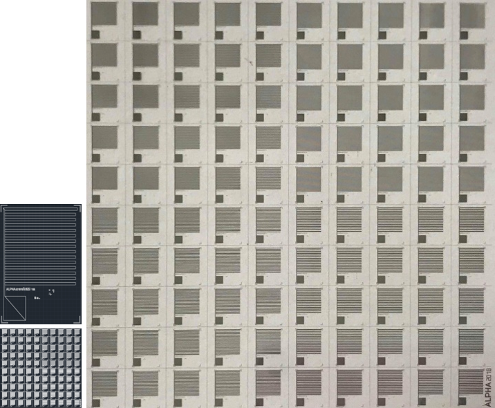
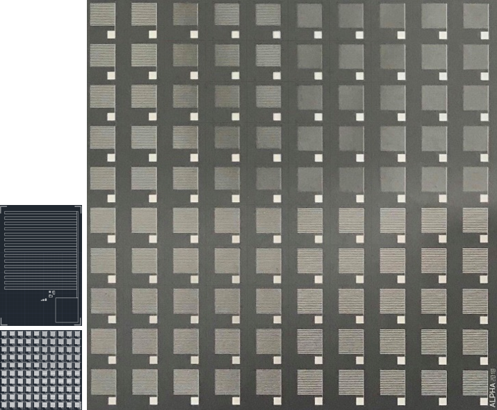
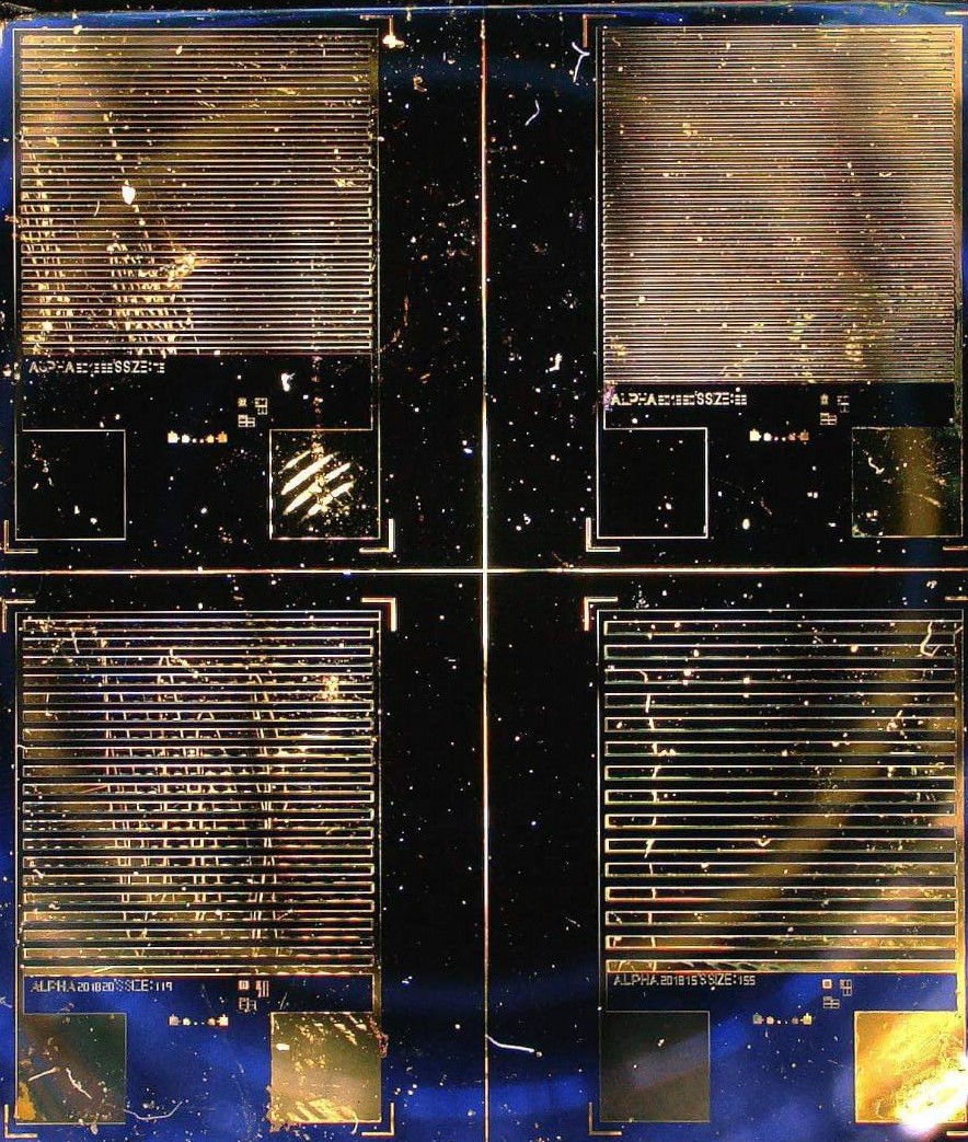
    First, the glass substrate with ITO was immersed in acetone at the ultrasonic for 5 min to remove the organic particles, then it was immersed in methanol at the ultrasonic for 5 min to remove acetone, then finally it was immersed in distill water (DI water) at ultrasonic for 5 min. Then the glass was dried by nitrogen blowing after completing the above clean process. Before device process, testing the resistance of two sides of sample to find the ITO layer is necessary. Then baking it for one5 min at onetwo0°C to prevent the residual -OH sites. The ITO layer was firstly applied HMDS to enhance PR adhesion, which performed in a spin coater with 3000 rpm for one0 s at one step to spray out the residue and 5000 rpm for two0 s at two step to control the thickness. Sending PR-coated ITO to do soft baking for two min at 90°C to let PR dried a little and enhance the adhesion. After a soft baking, exposing the pattern through the designed mask irradiating at a 365 nm ultraviolet light from a mercury lamp for two.5 s. A positive PR is chosen in the photolithography. The part opened in the mask, which is not covered by the hard mask of Cr, can be used to defined the illumination area. Photoresist with illumination should be baked after exposure for one min at 90°C to prevent erosion ripples around the chip before developing. Then, the chip was soaked in the developer, AZ300MIF, and shacked to remove the exposured photoresist. The remained PR has to be observed in an optical microscope. If the critical patterns matched to our designs then the device can be sent to do hard baking at onetwo0°C for one5 min. Soak the developed ITO in the etchant for approximately one0 min. The formula of etchant is hydrochloric acid 36%, nitric acid 70% and DI water with a ratio of 50:3:50. After wet etching process, the sample immersed in acetone and shack it to get rid of PR and the pattern of ITO electrode would be obtained clearly. Finally, the glass substrate printed with the first electrode was placed in a one00% acetone shake to remove the photoresist, and the first electrode on the chip was completed.

    After confirming the state of the first electrode by the optical microscope and alpha stepper, the process of the second electrode will be performed on the same chip. The chip was immersed in acetone at the ultrasonic for 5 min to remove the organic particles or dust, then it was immersed in methanol at the ultrasonic for 5 min to remove acetone, then finally it was immersed in DI water at ultrasonic for 5 min, which the chip was dried by nitrogen blowing. Baking at onetwo0°C for one5 min can be used to remove surface moisture and improve the adhesion to photoresist. Similar process of the first photolithography will be performed for the second photolithography for the lift off process of Au electrode. With the patterns designed in the mask and alignment to the electrodes in the first lithography, a inversed patterns of Au electrodes could be fabricated on chip surface by the photoresist. A Ti layer of one00 Å and a gold layer of approximately one500 – one600 Å is evaporated by a thermal evaporator. To have a high uniformity, the thermal evaporator system has to be pumped to high vacuum (~one0-6 torr). two tungsten boats are used to put Ti and Au material, which could be melt and evaporated with a high current passed through. With a monitor by QCM, the thickness of Ti and Au could be easily obtained by the current level and process time control. After evaporation, whole chip could be put in the acetone to remove the photoresist and the Ti/Au on it. Remained Ti/Au layer with the designed patterns could be transferred to chip to be the second electrodes.

    The way to make the electrodes is to perform the lithography process in the room which the light is yellow. The lithography is to temporarily coat the surface of the chip with photoresist, and design the mask to transfer the design pattern to the photoresist, which is the most important in chip manufacturing.

    We can produce several " FF " in once procession ( Fig3 ). There are four kinds of pattern which get the different distance between two electrodes.

    Fig.3 ( left ) Four kinds of " FF " pattern

    Fig.4 showed the real situation of the " FF " that we had made. Two elecctrodes were combined successfully in the lithography process.

    Fig.4 ( right ) Single " FF " pattern

    Fig.5 showed the distance between two electrodes, were measured as 3000 - 4000 nm. The result was not under our expection, therefore, we came out another idea - stacked electrodes.

    Fig.5 The distance of two electrodes in " FF " pattern

  • Stacked Electrodes
  • ×

    Stacked Electrodes


    The same process of Ti and Au layer deposition is performed in the chip as the first electrode. The graphene with the coated PMMA membrane is placed on the Au surface. PMMA membrane could be the insulator. Graphene could be the second electrode. The gap between Au and graphene, which is the thickness of PMMA, could be the distance between two electrodes. This simple structure could be used to test the DNA hybridization with two different surface immobilization on two different electrodes.

    As the lithography process is much more difficult to achieve the goal we set earlier. The distance of two electrodes could not be controlled accurately in every finger int the chip. Even 0.1 degree displacement would led the electrodes in the chip with 40 – 50 % error.

    Therefore, we used another method, stacking electrode, to test the connection between target and probe DNA instead.

    Discussion

  • The distance between two electrodes
  • If the distance between two electrodes is too long would not make the DNA bridge connect properly. We must keep a certain elastic space to prevent the single-strand DNA bending or distortion in the buffer causing connection problem. More probe DNA is one of the solutions; in other words, high-precision measurement by adding more target DNA to increase collision and connection opportunities with probe DNA. However, if the distance between two electrodes is too short, target DNA would directly touch the electrodes on both sides, causing the measurement error. We can't judge whether the cause of the conduction is the correct DNA connection, or just the DNA stuck on it.

  • The selection of material
  • In addition to good electrical conductivity and bio-connectivity, the choice of materials is also very important for the accuracy and convenience in the process. We used ITO as the material of the electrode, but the ITO is transparent, which cause considerable error in the result. The stability of the material is also one of the conditions considered. Even if the material has good conductivity, such as Cu, the oxidizing property makes it impossible to be the material of choice. Our ultimate goal is to make a POCT product, so the stability of material will directly affect the quality of the goods.

    Conclusion

    We have created a biosensor that is different from the previous one. Advanced from single electrode to double electrode, we chose Au and graphene to make electrodes. The largest difficulty in our ideal "FF" planar double electrode design is the control of the distance between two electrodes. The dense electrode and the electrode should be kept 2 μm, which requires precise alignment and long-time process. It is more complicated than the platform electrode, but the surface area is larger and can be connected with more target DNA is and is more sensitivity. Although the surface area of the platform electrode is reduced, the measurement method is the same as that of the planar electrode measurement. Therefore, due to the time, we will temporarily adopt the platform electrode as the final test measurement.

    © Copyright 2018 @CGU